科学研究
Research
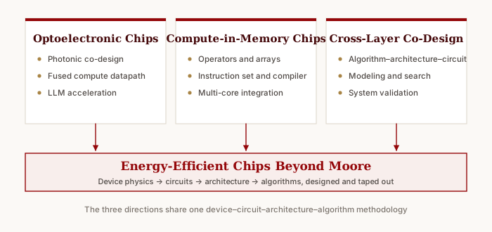
With Moore's law slowing, efficiency gains increasingly come from combining new devices with new architectures. The lab pursues three directions: optoelectronic fusion, compute-in-memory, and the cross-layer methodology that connects them.
Overview
The three directions are not independent. Optoelectronics and compute-in-memory provide two complementary physical substrates for computation; cross-layer co-optimization determines whether algorithms can actually use them.
I Optoelectronic chip architecture and circuit design
Electrical interconnect bandwidth and power are becoming the dominant bottleneck in large-model inference. Light propagates with almost no energy loss and naturally supports wavelength and spatial parallelism, but it is hard to store and hard to use for precise nonlinear operations. That complementarity argues not for all-optical computing but for letting each domain do what it does well.
What we work on
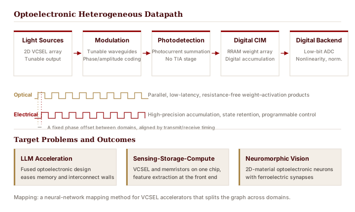
VCSEL arrays and memristor arrays sit on a single datapath: the optical domain performs highly parallel weight–activation products and long-distance data distribution, while the electrical domain handles precise accumulation, state retention and programmable control. Building that datapath raises problems at the device, circuit and compiler levels.
Specific topics
- Prototype photonic devices and circuits Supported by a National Key R&D "Matter Manipulation" project, exploring new optical field control mechanisms and abstracting device behaviour into compact models usable for circuit design. Search
- Optoelectronic fusion architecture for large language models Addressing the memory and interconnect walls in large-model inference with a co-designed compute and data distribution architecture, plus a mapping method that automatically partitions the compute graph between optical and electrical domains at compile time. Patent search
- Transimpedance-amplifier-free cascaded CIM circuits with RRAM and VCSEL Merging photodetection and in-memory multiply–accumulate into a single stage, cutting the noise and power overhead of inter-stage conversion. Patent search
- Sensing-storage-compute VCSEL chips and hardware systems With Vertilite, integrating light emission, detection and computation into one hardware system so that feature extraction happens at the sensing front end. Vertilite
- Neuromorphic vision devices and circuits Homogeneous integration of 2D-material optoelectronic neurons with ferroelectric synapses (Nature Communications 2026); configurable optical hetero-synapses based on full van der Waals bipolar ferroelectric structures for in-sensor computing (Advanced Materials 2024). Nature Commun. 2026Adv. Mater. 2024
- In-situ frequency conversion circuits Current-controlled VO2 device arrays perform signal synthesis and mixing in place, cutting end-to-end wireless IoT energy by 1.45–1.94× (Nature Communications 2024). DOI
II Compute-in-memory architecture and circuit design
Compute-in-memory already handles multiply–accumulate well, but real workloads are full of nonlinear operations, conditional logic and data movement — sorting, Fourier transforms, differential equation solving, database queries — which have had to fall back to digital logic and become the system bottleneck. Most of our work targets that class of operators.
In-memory operators: closing the operator gap
Sorting rests on comparison, which needs precise conditional logic and data movement; architectures designed for multiply–accumulate struggle with it. We proposed a comparator-free sorting circuit based on a bit-read mechanism that is compatible with existing matrix computation, achieving 3.3–7.7× speedup and 6.23–183.5× better energy efficiency than existing ASICs, and 7.7× higher speed than CMOS sorting circuits. Fourier transforms are implemented from first principles by heterogeneous volatile/non-volatile circuits: volatile devices generate the spectrum in situ while non-volatile devices perform the multiply–accumulate, supporting arbitrary radix, non-uniform and high-precision transforms at 504.3 GS/s, against roughly 100 GS/s for the fastest prior work.
Chips and systems
- Sub-10-millisecond neural dynamical system chip A controllable compute-in-memory paradigm on phase-change memristors: by exploiting conductance drift and multi-level conductance, the integration step is encoded directly as a device conductance state, enabling in-situ adaptive step search and multi-level in-memory multiply–accumulate. In 40nm, the CIM and step-drift arrays occupy 0.28 mm2 at 50 MHz, with 9 pipeline stages per integration step and 2.12 ms per iteration (Science 2026). DOIEurekAlert!
- Mixed-precision phase-change CIM chip for embodied AI 40nm, digital compute-in-memory with adaptive drift compensation, cutting programming latency by 63.3% and computation loss by 13.1×, reaching 0.821 TFLOPS/W (IEDM 2025). Search
- Dual-mode CIM architecture for neural manifolds Current-domain and charge-domain dual-mode design giving a 476× energy efficiency gain, used for neural manifold learning. IEDM 2024
- MeMCISA in-memory database instruction set A memory-centric instruction abstraction for database operations (MICRO 2024). Search
- Programmable probabilistic computing accelerator 42–1058× faster than GPUs on sampling-heavy tasks such as causal inference. HPCA 2025
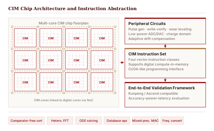
- CIM instruction set and end-to-end framework Four vector instruction classes form a complete operator set supporting digital compute-in-memory, exposing a CUDA-like interface. The validation framework is compatible with Huawei Kunpeng and Ascend simulators and has been deployed in Huawei's computing product line with up to 16.6× speedup.
- Array reliability circuits On-chip write-verify and endurance enhancement, wear levelling across multiple RRAM cores, and finite-state-machine write verification, supporting long-term stable operation of multi-level arrays.
III Algorithm–architecture–circuit co-optimization
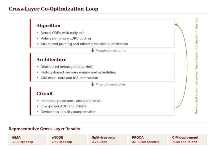
Whether new devices deliver depends on whether all three layers are optimised toward one objective. Change only the algorithm and the hardware cannot run it; change only the circuit and no algorithm can use it. This direction studies how the interfaces between layers should be defined.
Distributed heterogeneous networks-on-chip
For workloads ranging from neural networks to communication coding, we build distributed heterogeneous on-chip networks that break the concurrency bottleneck of AI chips. On the communication side, the first parallel split-tree polar coding architecture reached 3.25 Gbps, the highest throughput at the time, and a nonbinary LDPC parity-check architecture addressed the error-floor problem that long hindered LDPC deployment. On the AI side, the distributed HiMA architecture is 39.1× faster than the fastest AI chip of its time, the neural-ODE architecture with early exit gives 2.6× speedup, and a DNC-aided decoding architecture cuts latency by 54%.
Cross-layer methods
- Structured pruning and stepsize search Two-stage structured pruning with history-based stepsize search accelerates neural ODE inference on FPGAs (FPGA 2023). Search
- Mixed-precision quantization Nested dynamic mixed-precision quantization for mixture-of-experts models, allocating bit widths per expert and per layer.
- Hardware-aware algorithm design Column-skipping sorting, memristor-based trigonometric functions, and finite-field error-correction coding for CIM architectures, all redesigned from the physical behaviour of the devices and arrays. Column-skipping arXiv
- Accelerators for emerging workloads The MGPA single-cell RNA sequencing genome processing accelerator (DATE), cloth simulation acceleration, reservoir computing and seizure detection hardware. MGPA
- Stochastic and approximate computing A mixed-precision edge accelerator for embodied AI reaching 534.6 TOPS/W in 28nm. A-SSCC 2025
Research projects
The lab leads projects funded by the NSFC, the National Key R&D Program, the Beijing Natural Science Foundation and industrial partners, spanning fundamental mechanisms through to engineering deployment.
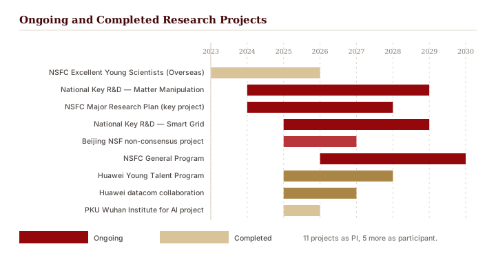
As principal investigator
| Funding source | Category | Project |
|---|---|---|
| NSFC | Excellent Young Scientists Fund (Overseas) | Hardware–software co-designed chip architecture with advanced devices |
| NSFC | General Program | High-concurrency neural-ODE compute-in-memory chips |
| NSFC | Major Research Plan key sub-project | Heterogeneous CIM architecture fusing SRAM and RRAM |
| Ministry of Science and Technology | National Key R&D, Matter Manipulation | Prototype photonic device construction |
| Ministry of Science and Technology | National Key R&D, Smart Grid | Sensing-storage-compute micro/nano sensing units: mechanisms and architecture |
| Ministry of Science and Technology | National Key R&D, Strategic S&T Cooperation | Bidirectional brain–computer interaction for mental health with large models and cognitive mechanisms |
| Beijing Natural Science Foundation | Non-consensus research project | Higher-order dynamical chip architecture beyond the Turing machine |
| PKU Wuhan Institute for AI | Technical collaboration | Vision compute-in-memory chip fusing memristors and SRAM |
| Huawei | Young Talent Program | Research on next-generation chip architecture |
| Huawei | Data communication product line | Low-power FEC technology |
| Vertilite | Technical collaboration | VCSEL sensing-storage-compute chip and hardware system |
As participant
- NSFC Major Research Plan: novel neuromorphic devices and neural network computing architecture based on memristor dynamics(completed)
- Beijing Natural Science Foundation–Changping Innovation Joint Fund: memristor compute-in-memory systems for renewable grid integration
- National Key R&D Program: large-scale, energy-efficient compute-in-memory systems
- US NSF FET Medium: Memory Processing Unit — An Efficient, Reconfigurable In-memory Computing Fabric(completed)
- US NSF CCF Small: Smart Continually-aware High-Fidelity Sensor Interfaces(completed)