Letting the physics of
beyond-Moore devices drive
computing performance
Beyond-Moore chip architecture and integrated circuit design
As Moore's law slows, performance no longer comes from smaller transistors alone. We redesign operator circuits, chip architectures and algorithm mappings on top of emerging devices, turning the physical behaviour of photonic and beyond-Moore devices directly into programmable computing capability — and we carry those designs all the way from simulation through tape-out to industrial deployment.
About the lab
The Lab for Emerging Architecture and Processor (LEAP-PKU) is based jointly in the School of Integrated Circuits and the Institute for Artificial Intelligence at Peking University, and is led by Prof. Yaoyu Tao.
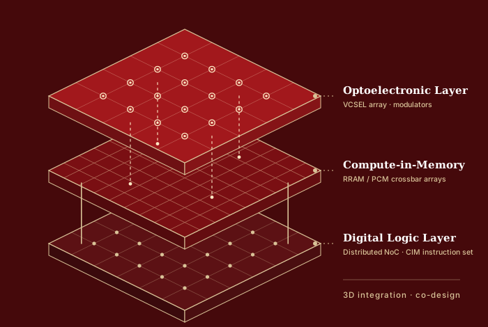
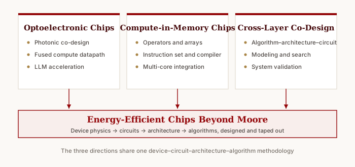
The lab works on one concrete question: when conventional digital circuits can no longer trade process scaling for efficiency, which computations can be handed to the devices themselves? Starting from bottleneck operators in AI and signal processing — Fourier transforms, sorting, frequency conversion, distance metrics — we build new operator circuits out of photonic and other beyond-Moore devices, then design the chip architecture and instruction abstraction that can schedule those operators, and finally verify the end-to-end gains through a full algorithm–architecture–circuit co-design flow. Results appear in Science, Nature Electronics and Nature Communications, as well as ISSCC, JSSC, VLSI, IEDM, MICRO, HPCA and FPGA; related circuit designs have reached volume production in chips at Huawei and other companies.
Direction I
Optoelectronic chip architecture
and circuit design
VCSEL arrays and memristor arrays are placed on a single datapath, with the optical domain performing highly parallel weight–activation products and the electrical domain handling precise accumulation and state retention. Read more
Direction II
Compute-in-memory architecture
and circuit design
In-memory circuits for nonlinear operators such as sorting, Fourier transforms and differential-equation solving, organised into a programmable multi-core chip by an instruction set built from four vector instruction classes. Read more
Direction III
Algorithm–architecture–circuit
co-optimization
Two-way constraints across algorithm, architecture and circuit: mapping requirements pass downward, device non-idealities feed back upward, so all three are optimised against one objective. Read more
Selected results
All of the following were led as first or corresponding author, spanning devices, circuits, architecture and systems.
- Sub-10-millisecond neural dynamical system chip (Science 2026) A controllable compute-in-memory paradigm built on phase-change memristors cuts single-step iteration latency to 2.12 ms and accelerates cortical reconstruction by 50–478× over advanced GPUs. Science published an accompanying perspective describing the work as a shift toward physics-driven computing. DOIEurekAlert!
- First-principles hetero-integrated Fourier transform system (Nature Electronics 2025) Volatile VO2 devices generate spectra in situ while non-volatile TaOx/HfOx devices perform the multiply–accumulate, supporting arbitrary radix and non-uniform transforms at 504.3 GS/s. DOI
- Reconfigurable sort-in-memory system (Nature Electronics 2025) The first comparator-free sorting circuit, built on a bit-read mechanism and compatible with existing matrix computation, giving 3.3–7.7× speedup and 6.23–183.5× better energy efficiency than existing ASICs. DOITechXplore
- MeMCISA in-memory database instruction set (MICRO 2024) Core database operations are pushed down into the memory array, forming a memory-centric instruction abstraction. Search
- HiMA history-based memory access engine (MICRO 2021) A distributed memory architecture for differentiable neural computers, 39.1× faster than the fastest AI chip at the time. arXiv
- Configurable split-tree polar decoder chip (VLSI 2019, JSSC 2021) 3.25 Gbps in 40nm, the highest throughput reported at the time; nominated for the VLSI best paper award. Search
Latest news
- September 2026 The programmable spatial optoelectronic heterogeneous AI inference chip was presented at the Pujiang Innovation Forum, and the Xingyao Yuedong team won first prize in the team category of the second Zhangjiang Cup Silicon Photonics Innovation and Entrepreneurship Competition. STAR Market DailyIT Times (reprint)All news
- July 2026 The neural dynamical system chip was published in Science and covered by People's Daily, Xinhua, Beijing Daily and others. DOIEurekAlert!
- January 2026 The hetero-integrated memristor Fourier transform system appeared in Nature Electronics. DOI
- December 2025 Three papers accepted at IEDM 2025, covering a mixed-precision phase-change CIM chip, a self-supervised learning accelerator and a multimodal fusion processor. Search